Measuring Control Systems

Kubota’s measurement business evolved from the optical, image processing, and precision machinery technologies we originally developed for our own in-house hard disk manufacturing. By integrating the optical, imaging, and precision mechanical expertise we have accumulated over the years, we now provide inspection systems that support manufacturing in cutting-edge industries, particularly the semiconductor and data storage sectors.
Our mission is to visualize the microscopic world invisible to the naked eye, helping our customers improve product quality. By detecting nanometer-scale defects and anomalies with high precision, we help prevent defective products from reaching the market, improve manufacturing yields, and ensure stable production.
Our flagship products include inspection systems for semiconductor wafers and hard disks. In semiconductor manufacturing, it is essential to detect and control minute defects during each process, such as circuit and wiring formation. Consequently, inspection systems play a critical role in determining both quality and productivity. As integration densities continue to rise, the demand for higher detection accuracy increases, making nanometer-scale detection the industry standard. Similarly, achieving high-density recording in hard disks requires extremely precise processing and assembly, where even the slightest anomaly can lead to data loss or device failure.
By providing optimal inspection solutions tailored to specific targets and manufacturing processes, Kubota is contributing to the growth of the electronic device industry, which serves as the backbone of today's global digital society.
- Product availability and specifications may vary by country or region. For more information, please contact the nearest Kubota from Global Network.
- To view more information about this product in your area, please select your country/region.
-
Select a country/area
Features
-
Inspection Technology Honed for Over 25 Years
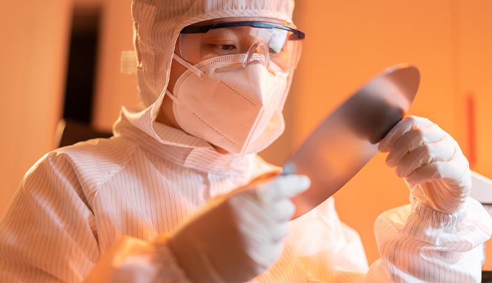
The roots of Kubota’s inspection system development lie in our own in-house hard disk manufacturing. Cultivated on the front lines of manufacturing where rigorous quality standards are essential, our inspection technologies soon became highly sought after by external customers, ultimately evolving into our current inspection systems business. Today, we leverage over 25 years of accumulated expertise in optics and image processing, alongside practical knowledge honed on the production floor, to provide advanced inspection systems to customers in both the semiconductor and hard disk industries.
-
Support for Transparent and Semi-Transparent Substrates Beyond Silicon
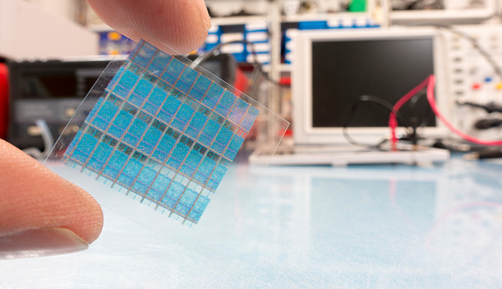
In addition to silicon, Kubota’s inspection systems support transparent and semi-transparent substrates such as SiC, sapphire, and glass. With transparent materials, light reflecting off the backside typically creates noise that makes it difficult to detect surface defects. However, Kubota utilizes a proprietary optical design to suppress this backside reflection. By scanning only the surface with high precision, we can reliably detect even the most minute defects. Because we can adapt our inspections to suit the specific materials used by our customers, we are well-equipped to meet the quality control needs of a wide range of industries.
-
Optimal Design Tailored to Inspection Processes and Production Environments
We provide our inspection systems only after thoroughly understanding our customers' inspection objectives, applications, and specific production environments. Rather than simply offering standard off-the-shelf specifications, Kubota conducts hands-on testing on actual machines using sample materials provided by the customer. This allows us to recommend the ideal features and specifications best suited to your specific inspection targets, criteria, and facility conditions. Because we deeply understand the yield improvement challenges faced on the front lines of semiconductor and hard disk manufacturing, we can design systems uniquely tailored to the individual requirements of every customer.

Lineup
Kubota offers a diverse lineup of semiconductor and hard disk (HD) inspection systems. Our portfolio includes laser-based systems that scan surfaces to detect minute defects, microscope-based systems utilizing differential interference contrast (DIC) microscopy, and hybrid models that integrate the strengths of both methods. Additionally, our lineup features models equipped with review functions that enable real-time observation and analysis via a laser microscope, as well as automated visual inspection systems designed to automate surface defect checks that previously relied on manual human inspection.
-
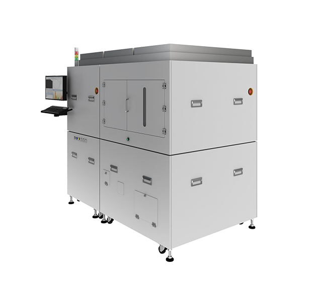
Wafer Surface Inspection System (Laser Type)
-
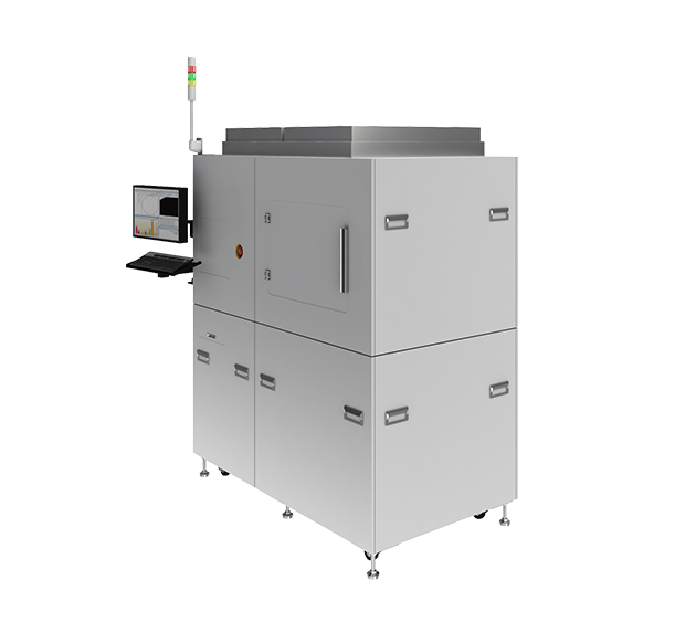
Wafer Surface Inspection System (Image Type)
-
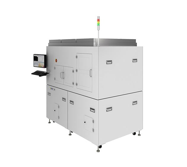
Wafer Surface Inspection System (Hybrid Type)
-
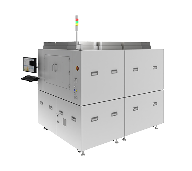
Wafer Surface Inspection System with Review Function
-
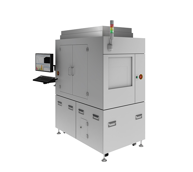
Wafer Visual Inspection System
-
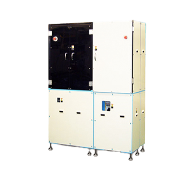
Laser Inspection System
-
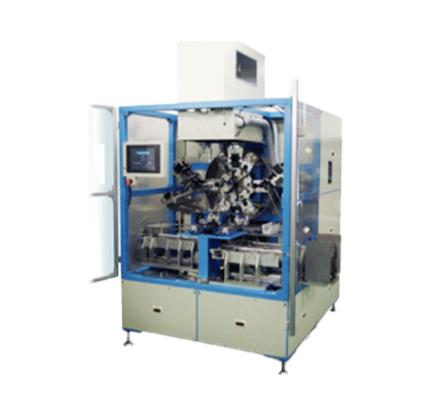
Disk Surface Inspection System
-
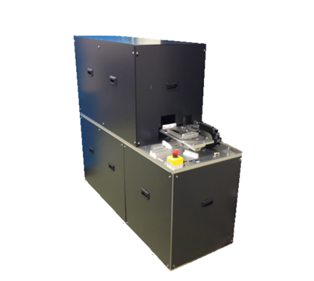
Visual Inspection System
Our Technologies
-
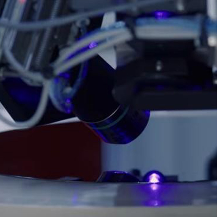
Optical Inspection Technology Based on Laser Scattering
This technology directs a high-power laser onto the wafer surface to detect, with exceptional sensitivity, the scattered light generated when the beam strikes a defect. By capturing this light through a multi-channel optical system, the system can scan the entire wafer surface at high speeds while ensuring that even the most microscopic defects are reliably detected.
-
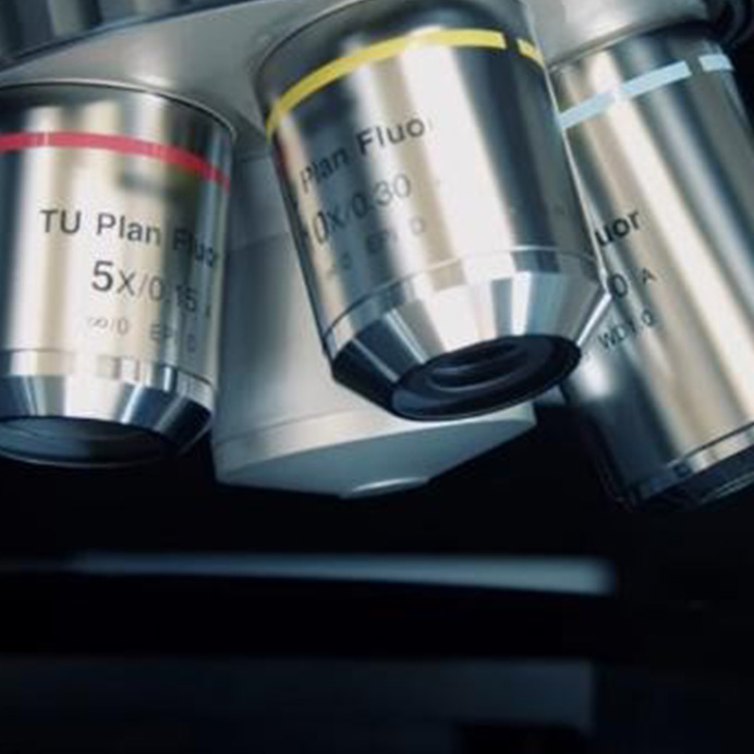
Image Processing Technology Utilizing Differential Interference Contrast (DIC) Microscopy
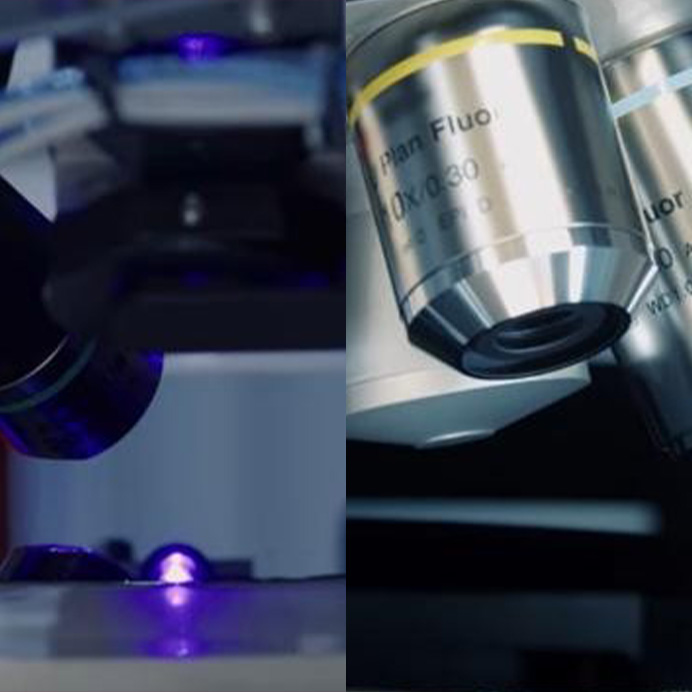
Differential Interference Contrast (DIC) microscopy is a technique that enhances and visualizes even the most minute surface irregularities. Kubota combines this technology with our proprietary image processing capabilities to capture full-surface images of the wafer while the stage is being scanned. We leverage these highly detailed images to determine the exact size and shape of defects and to conduct in-depth analyses.
-
Hybrid Technology Integrating Multiple Methods into a Single System
By combining the high-speed inspection capabilities of laser-based systems with the detailed microscopic defect analysis of microscope-based systems, we have developed hybrid machines capable of completing both inspection and analysis within a single unit. We also offer models equipped with a review function utilizing an integrated laser microscope, enabling a highly efficient workflow from the initial inspection to the detailed verification of defects.
-
Automated Visual Inspection Systems
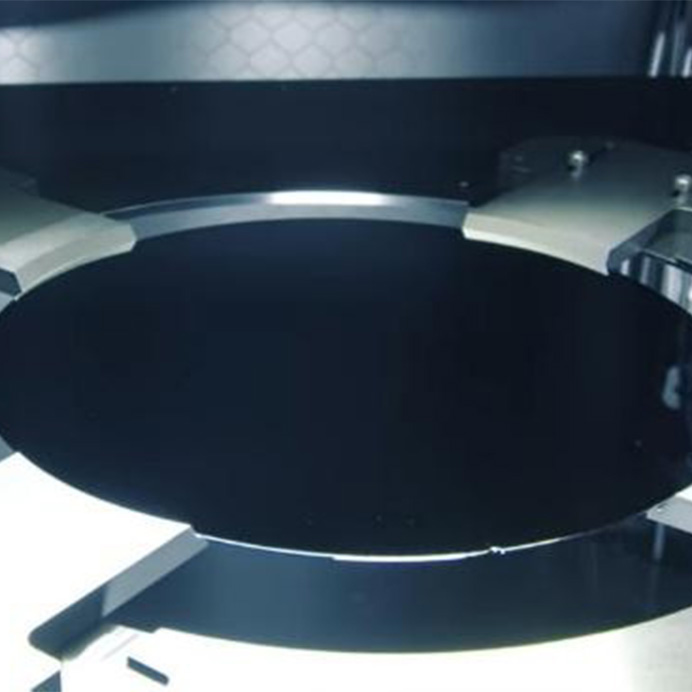
By automating not only defect detection but also the classification of defect shapes and types, these systems help reduce the workload required for reviewing inspection results and ensure highly consistent quality assessments. To guarantee the highest level of accuracy in this classification, we also leverage AI technology as needed.
- To view more information about this product in your area, please select your country/region.
-
Select a country/area

